
The addition of tomographic capability builds on RPM technology that has broken new ground in taking AFM from Lab to Fab with launch of the Metron3D.
Using existing features of the design in new ways has enabled further innovation, providing 3D tomographic capability for semiconductor characterization. The system uses multiple probes to generate sub-nanometre resolution 3D map of conductivity and geometry that can provide powerful insights in the development of new device architectures.
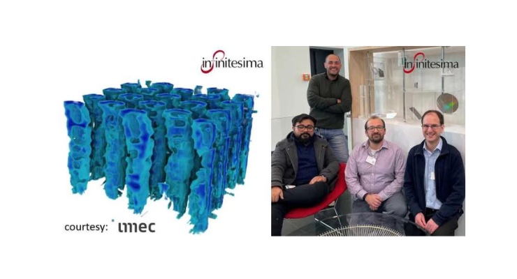
Today’s semiconductor devices use complex 3D structures to achieve high density and high performance, with feature dimensions of just a few nanometres. When a device fails it can be challenging to determine the root cause, whether it’s particle contamination, dopants, or voids in the structure.
The ability to generate sub-nanometre resolution 3D maps of both the device geometry and the local electrical properties enables straightforward visualisation and identification of these defect sources.
To realize this capability, Infinitesima its extending their joint development program (JDP) with imec.
“We are very proud to be continuing our work with imec to commercialise their pioneering research,” said Peter Jenkins, CEO of Infinitesima. “To continue Moore’s law there is a transition towards ever smaller and more complex 3D device structures. Current characterization and metrology methods are reaching their limits and we need new solutions now to enable the technology of tomorrow.”